代碼工程的GITHUB連接:
https://github.com/sj15712795029/stm32f1_marvell88w8801_marvell8801_wifi
Marvell自己實現驅動系列文章分為幾篇介紹:
每篇更新打開專欄可以看到:
在介紹SDIO協議之前,我們來看下Wi-Fi市面上的種類
市面上大致有這幾種Wi-FI,其中優缺點也是我個人簡介,大家一看就好,至于有不同意見,可以交流
1)UART WIFI,以ESP8266為代表,主要實現方式是芯片內集成了wifi driver tcp/ip protocol rtos memory IC等等,讓你可以直接AT命令控制芯片
優點:使用便利,開發者不需要懂WIFI driver,TCP/IP protocol,RTOS的概念
缺點:功能受限,可定制化比較低,需要外掛一個MCU
另外,ESP8266也分為AT板和SDK板,SDK也可以克服以上缺點,但是我沒有使用過SDK,所以不能胡說錯誤的引導你們
2)SDIO WIFI
3)USB WIFI
其中SDIO和USB市面上就比較多了,大部分的Wifi芯片都是以上兩種接口,Marvell88w8801支持USB2.0和SDIO2.0 ,USB wifi大家看名字應該就能想象到時什么東西,就是類似于一個USB dongle,下圖模樣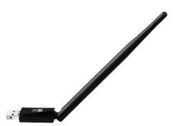
SDIO WIFI我們后續會介紹,所以大家不要急
4)PCIE WIFI如圖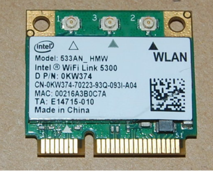
5)OPENWRT WIFI
由于我沒有做過這個,所以不做評論
做一個簡短性的話語總結,SDIO有分為FUNC的概念,你可以把FUNC比作功能區,FUNC0是每個SDIO card必須實現的,FUNC1~7是可選存在的,一般的WIFI card會實現FUNC1,在每個FUNC中又會有寄存器的概念,FUNC0中的寄存器地址是SDIO協議規定,FUNC1~FUNC7中的寄存器地址是vendor(芯片廠商)去實現的,所以要訪問一個地址的數據,首先要告知FUNC,然后再告知register address,整個大背景在這,好啦,SDIO講解到此為止~哈哈,玩笑啦,帶著這些去讀下面的內容吧,會讓你更容易理解
SDIO設備的硬件操作接口有3種方式:
A、 SPI mode;
B、 SD 1-bit mode;
C、 SD 4-bit mode;
這3種方式的硬件接口及管腳定義如下面圖、表: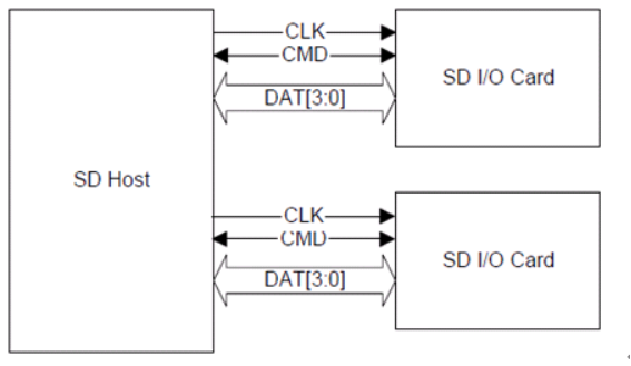
圖1 SDIO硬件接口(連接了2組sdio設備)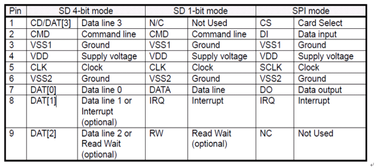
表1 SDIO各種模式管腳對應關系
本文不對SPI mode的相關內容介紹,有關SPI mode的內容不做過多說明。
2.2.1 Common I/O Area (CIA)
The Common I/O Area (CIA) shall be implemented on all SDIO cards. The CIA is accessed by the host via I/O reads and writes to function 0. The registers within the CIA are provided to enable/disable the operation of the I/O function(s), control the generation of interrupts and optionally load software to support the I/O
functions. The registers in the CIA also provide information about the function(s) abilities and requirements. There are three distinct register structures supported within the CIA. They are:
1) Card Common Control Registers (CCCR)
2)Function Basic Registers (FBR)
3)Card Information Structure (CIS)
如圖所示,就是FUNC0的CIA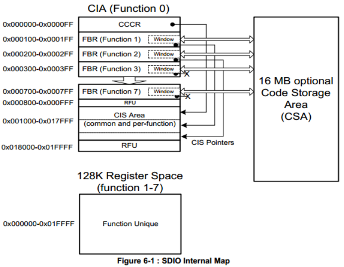
下面我們來一一介紹CCCR,FBR,CIS
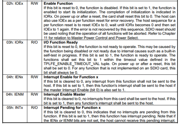
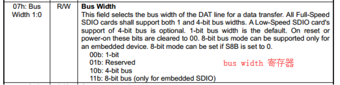
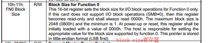
Card Common Control Registers (CCCR):CCCR說白了就是FUNC0的一些寄存器,地址和功能如下,另外,如果把所有的都列出內容實在太多,在這里只是列舉一些重要的,如果想獲取所有的功能,請自行參考SDIO協議: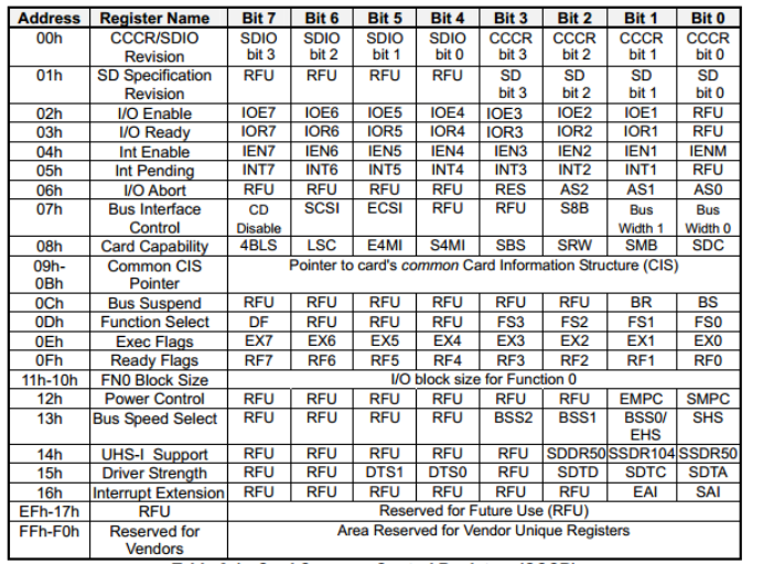

2.2.2 Function Basic Registers (FBR)
In addition to the CCCR, each supported I/O function has a 256-byte area used to allow the host to quickly determine the abilities and requirements of each function, enable power selection for each function and to enable software loading. The address of this area is from 00n00h to 00nFFh where n is the function number (1 to 7). This per-function area is structured as follows: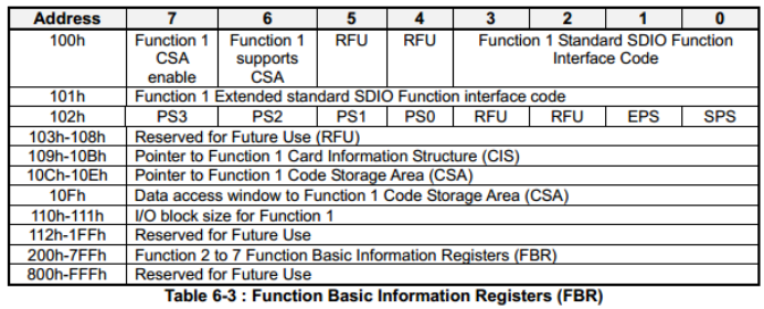
2.2.3 Card Information Structure (CIS)
The Card Information Structure provides more complete information about the card and the individual functions. The CIS is the common area to read information about all I/O functions that exist in a card. The design is based on the PC Card16 design standardized by PCMCIA. All cards that support I/O shall have a common CIS and a CIS for each function. The CIS is accessed by reads to a fixed area as shown in Table 6-5 This one area serves the card as a Common CIS and also as the storage area for each function. The common area and each function have a pointer to the start of its CIS within this memory space.
另外,CIS是tuple實行存在的,所以如果讀出來需要自己解析,在后面小節會抽出一章節講解tuple.
2.2.4 SDIO 命令/相應介紹
SDIO spec中有提到幾點SDIO card必須要實現的以及可選要實現的命令,如下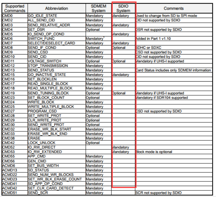
必須要實現的有:CMD0,CMD3,CMD5,CMD7,CMD15,CMD52,CMD53
可選實現的有:CMD8,CMD11,CMD15
Marvell88w8801的datasheet上也有說這顆芯片支持的CMD,算是把強制需要support的都做了,選擇支持的一個沒做,哈哈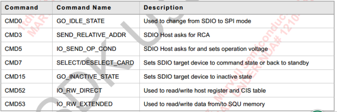
但是我們一般用到的有CMD0,CMD3,CMD5,CMD7,CMD52,CMD53,所以以這幾個命令來做簡短說明
1)CMD0:用于從SDIO mode切換到SPI mode
2)CMD3:詢問相對可用地址,response是R6
代碼如下:
/******************************************************************************
 *	函數名:	hw_sdio_cmd3
 * 參數:  	para(IN)		-->發送cmd3的參數
 			resp			-->cmd3的返回值
 * 返回值: 	返回執行結果
 * 描述:	發送cmd3
******************************************************************************/
static uint8_t hw_sdio_cmd3(uint32_t para,uint32_t *resp)
{
    uint8_t error_status;
    uint32_t response;
    SDIO_CmdInitTypeDef SDIO_CmdInitStructure;

    SDIO_CmdInitStructure.SDIO_Argument = para;
    SDIO_CmdInitStructure.SDIO_CmdIndex = SDIO_CMD3;
    SDIO_CmdInitStructure.SDIO_Response = SDIO_Response_Short;
    SDIO_CmdInitStructure.SDIO_Wait = SDIO_Wait_No;
    SDIO_CmdInitStructure.SDIO_CPSM = SDIO_CPSM_Enable;
    SDIO_SendCommand(&SDIO_CmdInitStructure);

    /* 等待發送完成 */
    while (SDIO_GetFlagStatus(SDIO_FLAG_CMDACT) == SET);
    error_status = hw_sdio_check_err();

    if (HW_ERR_OK != error_status)
    {
        return error_status;
    }

    /* 獲取到response的結果 */
    response = SDIO_GetResponse(SDIO_RESP1);
    if (resp)
    {
        *resp = response;
    }

    return (error_status);
}
R6的格式格式為,只有紅框內的數據才是軟件可以獲取的,其他的都是交于硬件去搞定
Bit 0~15是card status,如下圖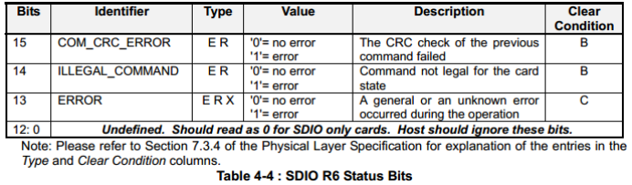
Bit 16~31就是我們獲取的相對地址,需要軟件解析出來,搭配CMD7來使用
解析代碼如下:
/******************************************************************************
 *	函數名:	hw_sdio_parse_r6
 * 參數:  	r6(IN)			-->R6的入參
 			rca(OUT)		-->rca的返回值
 * 返回值: 	返回執行結果
 * 描述:	解析R6的response
******************************************************************************/
static uint8_t hw_sdio_parse_r6(uint32_t r6,uint32_t *rca)
{
    HW_ENTER();
    if(rca)
    {
        *rca = RCA_IN_R6(r6);
        HW_LEAVE();
        return HW_ERR_OK;
    }
    HW_LEAVE();
    return HW_ERR_SDIO_INVALID_PARA;
}
3)CMD5, It is used to inquire about the voltage range needed by the I/O card.命令格式如下
Stuff Bits: Not used, shall be set to 0.
S18R: Switching to 1.8V Request
I/O OCR: Operation Conditions Register. The supported minimum and maximum values for VDD. The layout of the OCR is shown in Table 3-1. Refer to Section 4.10.1 for additional information
OCR如下圖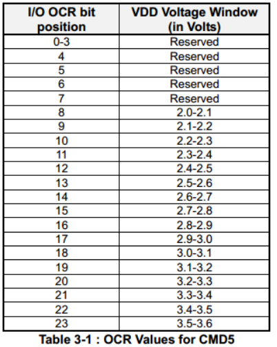
CMD5的response如下圖:
C: Set to 1 if Card is ready to operate after initialization
Number of I/O Functions: Indicates the total number ofI/O functions supported by this card. The range is 0-7. Note that the common area present on all I/O cards at Function 0 is not included in this count. The I/O functions shall be implemented sequentially beginning at function 1.
Memory Present: Set to 1 if the card also containsSD memory. Set to 0 if the card is I/O only.
S18A: Switching to 1.8V Accepted (Supported in SD mode only)
I/O OCR: Operation Conditions Register.
代碼如下:
/******************************************************************************
 *	函數名:	hw_sdio_cmd5
 * 參數:  	para(IN)			-->入參
 			resp(OUT)			-->返回值
 			retry_max(IN)		-->最大嘗試次數
 * 返回值: 	返回執行結果
 * 描述:	發送cmd5
******************************************************************************/
static uint8_t hw_sdio_cmd5(uint32_t para,uint32_t *resp,uint32_t retry_max)
{
    uint32_t index;
    uint32_t response;
    uint8_t error_status;
    SDIO_CmdInitTypeDef SDIO_CmdInitStructure;

    HW_ENTER();
    SDIO_CmdInitStructure.SDIO_Argument = para;
    SDIO_CmdInitStructure.SDIO_CmdIndex = SDIO_CMD5 ;
    SDIO_CmdInitStructure.SDIO_Response = SDIO_Response_Short;
    SDIO_CmdInitStructure.SDIO_Wait = SDIO_Wait_No;
    SDIO_CmdInitStructure.SDIO_CPSM = SDIO_CPSM_Enable;
    for (index = 0; index < retry_max; index  )
    {
        SDIO_SendCommand(&SDIO_CmdInitStructure);
        /* 等待發送完成 */
        while (SDIO_GetFlagStatus(SDIO_FLAG_CMDACT) == SET);
        error_status = hw_sdio_check_err();

        if (HW_ERR_OK != error_status)
        {
            continue;
        }
        response = SDIO_GetResponse(SDIO_RESP1);

        /* 判斷是否OK */
        if(C_IN_R4(response))
        {
            if (resp)
            {
                *resp = response;
            }
            break;
        }
    }

    HW_LEAVE();
    return error_status;
}
4)CMD7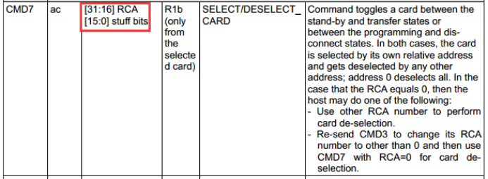
代碼如下:
/******************************************************************************
 *	函數名:	hw_sdio_cmd7
 * 參數:  	para(IN)			-->入參
 			resp(OUT)			-->返回值
 * 返回值: 	返回執行結果
 * 描述:	發送cmd7
******************************************************************************/
static uint8_t hw_sdio_cmd7(uint32_t para,uint32_t *resp)
{
    uint8_t error_status;
    uint32_t response;
    SDIO_CmdInitTypeDef SDIO_CmdInitStructure;

    HW_ENTER();
    /* Send CMD7 SDIO_SEL_DESEL_CARD */
    SDIO_CmdInitStructure.SDIO_Argument = para;
    SDIO_CmdInitStructure.SDIO_CmdIndex = SDIO_CMD7;
    SDIO_CmdInitStructure.SDIO_Response = SDIO_Response_Short;
    SDIO_CmdInitStructure.SDIO_Wait = SDIO_Wait_No;
    SDIO_CmdInitStructure.SDIO_CPSM = SDIO_CPSM_Enable;
    SDIO_SendCommand(&SDIO_CmdInitStructure);

    /* 等待發送完成 */
    while (SDIO_GetFlagStatus(SDIO_FLAG_CMDACT) == SET);
    error_status = hw_sdio_check_err();

    if (HW_ERR_OK != error_status)
    {
        return error_status;
    }
    /* 獲取返回結果 */
    response = SDIO_GetResponse(SDIO_RESP1);
    if (resp)
    {
        *resp = response;
    }

    HW_ENTER();
    return (error_status);
}
5)CMD52:CMD52是一個使用頻率很高的CMD,主要是用于讀寫SDIO的寄存器的命令
The IO_RW_DIRECT is the simplest means to access a single register within the total 128K of register space in any I/O function, including the common I/O area (CIA). This command reads or writes 1 byte using only 1 command/response pair. A common use is to initialize registers or monitor status values for I/O functions. This command isthe fastest means to read or write single I/O registers, as it requires only a single command/response pair.
命令格式如下,紅框內飾軟件需要實現的東西,其他的交給硬件:
R/W Flag: This bit determines the direction of the I/O operation. If this bit is 0, this command
shall read data from the SDIO card at the address specified by the Function Number and the Register Address to the host. The data byte is returned in the response, R5. If this bit is set to 1, the command shall write the bytes in the Write Data field to the I/O location addressed by the Function Number and the Register Address. If the RAW flag is 0, then the data inthe register that was written shall be read and that value returned in the response.
RAW Flag: The Read after Write flag. If this bit isset to 1 and the R/W flag is set to 1, then the
command shall read the value of the register after the write. This is useful to allow writing to a control register and reading the status at the same address. If this bit is cleared, the value returned in the R5 response shall be the same as the write data in the command. If this bit is set, the data field of the R5 response shall contain the value read from the addressed register after the write operation.
Function Number: The number of the function within the I/O card you wish to read or write. Note that function 0 selects the common I/O area (CIA).
Register Address: This is the address of the byte ofdata inside of the selected function to read or write. There are 17 bits of address available so the register is located within the first 128K
(131,072) addresses of that function.
Write Data/Stuff Bits: For a direct write command (R/W=1),this is the byte that iswritten to the selected address. For a direct read (R/W=0), this field is not used and shall be set to 0
響應類型:
Stuff Bits Not used, shall be set to 0
Response Flags 8 Bits of flag data indicating the status of the SDIO card. Table 5-1 shows the format of these flag bits.
Read or Write Data: For an I/O write (R/W=1) with the RAW Flag set (RAW=1) this field shall contain the value read from the addressed register afterthe write of the data contained in the
command. Note that in this case, the read-back data may not be the same as the data written to the register, depending on the design of the hardware. For an I/O write with the RAW bit=0, the SDIO function shall notdo a read after write operation, and the data in this field shall be identical to the data byte in the write command. For an I/O read (R/W=0), the actual value read from that I/O location is returned in this field.
代碼如下:
/******************************************************************************
 *	函數名:	hw_sdio_cmd52
 * 參數:  	write(IN)			-->執行操作,read or write
 			func_num(IN)		-->func的編號
 			address(IN)		-->address地址
 			para(IN)			-->要寫的參數
 			resp(OUT)			-->讀要返回的數據
 * 返回值: 	返回執行結果
 * 描述:	執行CMD52的動作
******************************************************************************/
uint8_t hw_sdio_cmd52(uint8_t write,uint8_t func_num,uint32_t address,uint8_t para,uint8_t *resp)
{
    uint8_t error_status;
    uint8_t response;
    SDIO_CmdInitTypeDef SDIO_CmdInitStructure;

    SDIO_CmdInitStructure.SDIO_Argument = write ? 0x80000000 : 0x00000000;
    SDIO_CmdInitStructure.SDIO_Argument |= func_num << 28;
    SDIO_CmdInitStructure.SDIO_Argument |= (write && resp) ? 0x08000000 : 0x00000000;
    SDIO_CmdInitStructure.SDIO_Argument |= address << 9;
    SDIO_CmdInitStructure.SDIO_Argument |= para;

    SDIO_CmdInitStructure.SDIO_CmdIndex = SDIO_CMD52;
    SDIO_CmdInitStructure.SDIO_Response = SDIO_Response_Short;
    SDIO_CmdInitStructure.SDIO_Wait = SDIO_Wait_No;
    SDIO_CmdInitStructure.SDIO_CPSM = SDIO_CPSM_Enable;

    SDIO_SendCommand(&SDIO_CmdInitStructure);
    /* 等待發送完成 */
    while (SDIO_GetFlagStatus(SDIO_FLAG_CMDACT) == SET);
    error_status = hw_sdio_check_err();

    if (HW_ERR_OK != error_status)
    {
        return  HW_ERR_SDIO_CMD52_FAIL;
    }

    response = SDIO_GetResponse(SDIO_RESP1) & 0xff;
    if((!write) && resp)
    {
        *resp = response;
    }
    return  HW_ERR_OK;
}
6)CMD53:同樣是一個高頻使用的CMD,主要用于對某一個地址進行多數據寫入或者多數據讀出的CMD,此命令分為兩種模式:block mode和byte mode,block mode必須是寫入或者讀出block size整數倍的數據,byte mode是可以寫入或者讀出任意大小的數據
命令格式:
R/W Flag: This bit determines the direction of the I/O operation. If this bit is 0, this command
reads data from the SDIO card at the address specified by the Function Number and the Register Address to the host. The read data shall be returned on the DAT[x] lines. If this bit is set to 1, the command shall write the bytes from the DAT[x] lines to the I/O location addressed by the Function Number and the Register Address.
Function Number: The number of the function within the I/O card you wish to read or write. Note that function 00h selects the common I/O area (CIA).
Block Mode (Optional) this bit, if set to 1, indicates that the read or write operation shall be performed on a block basis, rather than the normal byte basis. If this bit is set, the Byte/Block count value shall contain the number of blocks to be read/written. The block size for functions 1-7 is set by writing the block size to the I/Oblock size register in the FBR (Refer to Table 6-3 and Table 6-4). The block size for function 0 is set by writing to the FN0 Block Size register in the CCCR. Card and hostsupport of the block I/O mode is optional. The host can determine if a card supports block I/O by reading the Card supports MBIO bit (SMB) in the CCCR (Refer to Table 6-2). The block size used when Block Mode = 1 and the maximum byte count per command used when
Block Mode = 0 can be read from the CIS inthe tuple TPLFE_MAX_BLK_SIZE (Refer to Section 16.7.4) on a per-function basis.
OP code Defines the read/write operation as described in Table 5-2
? OP Code 0 is used to read or write multiplebytes of data to/from a single I/O register address. This command is useful when I/O data is transferred using a FIFO inside of the I/O card. In this case, multiple bytes of data are transferred to/from a single register address. For this operation, the address of the register is set into the Register Address field. Data is transferred on the DAT[0] orDAT[3:0] lines as defined for SD memory cards.
?OP Code 1 is used to read or write multiple bytes of data to/from an I/O register address that increment by 1 after each operation. This command is used when large amounts of I/O data exist within the I/O card ina RAM like data buffer. In this operation,the start address is loaded into the Register Address field. The first operation occurs at that address within the I/O card. The next operation shall occur at address 1 with the address incrementing by 1 until the operation has completed. As with OP Code 0, the number of bytes is set in the Byte Count field of the command.
Register Address: Start Address of I/O register to read or write. Range is [1FFFFh:0]
Byte/Block Count :If the command is operating on bytes (Block Mode = 0), this field contains the number of bytes to read or write. A value of 000h shall cause 512 bytes to be read or written.
If the command is in block mode (Block Mode=1), the Block Count field specifies the number of Data Blocks to be transferred following this command. A value of 000h indicates that the count set to infinite. In this case, the I/O blocks shall be transferred until the operation is aborted by writing to the I/O abort function select bits (ASx) in the CCCR (Refer to Table 6-1 and Table 6-2). Table 5-3 shows the relationship between the value in the command and the actual number of bytes transferred.
代碼如下:
/******************************************************************************
 *	函數名:	hw_sdio_cmd52
 * 參數:  	write(IN)			-->執行操作,read or write
 			func_num(IN)		-->func的編號
 			address(IN)			-->address地址
 			incr_addr(IN)		-->地址是否累加
 			buf(IN/OUT)			-->如果操作是寫,那么此參數就是要write的buffer
 									如果操作是讀,那么此參數就是read返回的buffer
 			size(IN)			-->讀或者寫的size
 * 返回值: 	返回執行結果
 * 描述:	執行CMD53的動作
******************************************************************************/
uint8_t hw_sdio_cmd53(uint8_t write, uint8_t func_num,uint32_t address, uint8_t incr_addr, uint8_t *buf,uint32_t size)
{
    uint16_t func_cur_blk_size;

    if((phw_sdio_core->func)[func_num])
    {
        func_cur_blk_size = (phw_sdio_core->func)[func_num]->cur_blk_size;
        if(func_cur_blk_size == 0)
        {
            return HW_ERR_SDIO_BLK_SIZE_ZERO;
        }
    }
    else
    {
        return HW_ERR_SDIO_INVALID_FUNC_NUM;
    }

    if(write)
    {
        /* CMD53 write */
        hw_sdio_cmd53_write(func_num,address,incr_addr,buf,size,func_cur_blk_size);
    }
    else
    {
        /* CMD53 read */
        hw_sdio_cmd53_read(func_num,address,incr_addr,buf,size,func_cur_blk_size);
    }

    return  HW_ERR_OK;
}
2.2.5 SDIO init介紹
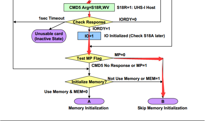
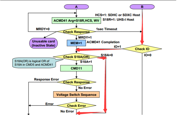
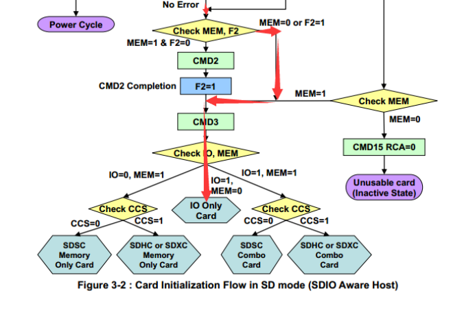
關于SDIO init流程,我們先以一個圖示介紹,由于此圖示是結合SD memroy card一起的,所以我們在圖中以箭頭表示流程,如圖所示: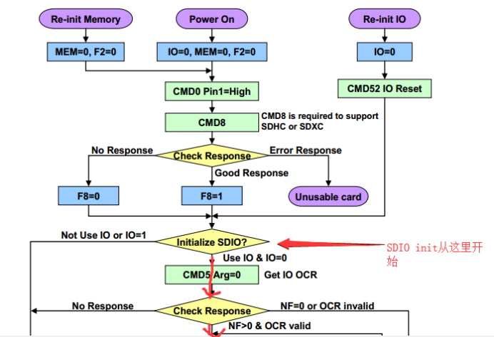
其中有一些術語如圖所示: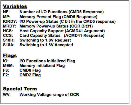
大概過程如下:
1)發送CMD5沒有參數,主要用于獲取OCR的范圍
2)FUNC的數目和OCR如果合法那么就重新發送CMD5,帶著OCR的參數
3)得到RESPONSE后,查看MP的filed,正常來說SDIO MP應該為0,所以走B case
4)B case下IO為1,并且S18為0,所以直接走CMD3,然后是IO=1,MEM=0,也就是SDIO整個初始化完畢,但是SDIO還有一些其他選項需要做,比如選擇SDIO設備,讀取一些CCCR的信息,切換SDIO bus width,提高SDIO CLK,解析CIS,設置BLOCK size之類的,下面我貼出我在STM32寫的代碼,僅供參考流程,這部分也在我的GITHUB能找到
/******************************************************************************
 *	函數名:	hw_sdio_init
 * 參數:  		NULL
 * 返回值: 	返回執行結果
 * 描述:		SDIO init
 				pin腳分配
 				PC8->SDIO D0 PC9->SDIO D1 PC10->SDIO D2 PC11->SDIO D3
 				PC12->SDIO CLK
 				PD2->SDIO CMD
******************************************************************************/
uint8_t hw_sdio_init()
{
    uint32_t rca;
    uint8_t func_index;
    uint32_t cmd3_para;
    uint32_t cmd3_resp;
    uint32_t cmd5_para;
    uint32_t cmd5_resp;
    uint32_t cmd7_para;
    uint32_t cmd7_resp;

    GPIO_InitTypeDef GPIO_InitStructure;
    SDIO_InitTypeDef SDIO_InitStructure;
    //NVIC_InitTypeDef NVIC_InitStructure;

    HW_ENTER();
    hw_chip_reset();
    hw_sdio_core_init();
    /* 使能GPIO C/D的RCC時鐘 */
    RCC_APB2PeriphClockCmd(RCC_APB2Periph_GPIOC | RCC_APB2Periph_GPIOD, ENABLE);
    /* 使能SDIO RCC時鐘*/
    RCC_AHBPeriphClockCmd(RCC_AHBPeriph_SDIO, ENABLE);
    /* 使能DMA2時鐘,SDIO的DMA在DMA2 CHANNEL 4 */
    RCC_AHBPeriphClockCmd(RCC_AHBPeriph_DMA2, ENABLE);

    /* 設置推挽復用 */
    GPIO_InitStructure.GPIO_Pin = GPIO_Pin_8 | GPIO_Pin_9 | GPIO_Pin_10 | GPIO_Pin_11 | GPIO_Pin_12;
    GPIO_InitStructure.GPIO_Speed = GPIO_Speed_50MHz;
    GPIO_InitStructure.GPIO_Mode = GPIO_Mode_AF_PP;
    GPIO_Init(GPIOC, &GPIO_InitStructure);

    GPIO_InitStructure.GPIO_Pin = GPIO_Pin_2;
    GPIO_Init(GPIOD, &GPIO_InitStructure);

    /* SDIO初始化,CLK:400KHZ,數據寬度:1 bus */
    SDIO_DeInit();
    /* HCLK = 72MHz, SDIOCLK = 72MHz, SDIO_CK = HCLK/(178   2) = 400 KHz */
    SDIO_InitStructure.SDIO_ClockDiv = SDIO_CLK_400KHZ;
    SDIO_InitStructure.SDIO_ClockEdge = SDIO_ClockEdge_Rising ;
    SDIO_InitStructure.SDIO_ClockBypass = SDIO_ClockBypass_Disable;
    SDIO_InitStructure.SDIO_ClockPowerSave = SDIO_ClockPowerSave_Disable;
    SDIO_InitStructure.SDIO_BusWide = SDIO_BusWide_1b;
    SDIO_InitStructure.SDIO_HardwareFlowControl = SDIO_HardwareFlowControl_Disable;
    //SDIO_InitStructure.SDIO_HardwareFlowControl = SDIO_HardwareFlowControl_Enable;
    SDIO_Init(&SDIO_InitStructure);

    /* 設置為SDIO I/O模式 */
    SDIO_SetSDIOOperation(ENABLE);
    /* Set Power State to ON */
    SDIO_SetPowerState(SDIO_PowerState_ON);
    /* Enable SDIO Clock */
    SDIO_ClockCmd(ENABLE);

    /* 設置SDIO中斷,搶占優先級為3,相應優先級為4 */
#if 0
    NVIC_InitStructure.NVIC_IRQChannel = SDIO_IRQn;
    NVIC_InitStructure.NVIC_IRQChannelPreemptionPriority = WIFI_PREE_PRIO;
    NVIC_InitStructure.NVIC_IRQChannelSubPriority = WIFI_SUB_PRIO;
    NVIC_InitStructure.NVIC_IRQChannelCmd = ENABLE;
    NVIC_Init(&NVIC_InitStructure);
    SDIO_ITConfig(SDIO_IT_CCRCFAIL |SDIO_IT_DCRCFAIL | SDIO_IT_CTIMEOUT |\
                  SDIO_IT_DTIMEOUT | SDIO_IT_TXUNDERR |SDIO_IT_RXOVERR | \
                  SDIO_IT_STBITERR|SDIO_IT_SDIOIT, ENABLE);
#endif
    /* 開啟SDIO的DMA,此位置尤其重要,如果在CMD53中每次開啟,那么會DMA lock住 */
    SDIO_DMACmd(ENABLE);

    /* 發送cmd5 */
    cmd5_para = 0;
    if(hw_sdio_cmd5(cmd5_para,&cmd5_resp,SDIO_RETRY_MAX))
    {
        HW_LEAVE();
        return HW_ERR_SDIO_CMD5_FAIL;
    }

    /* ocr 3.2V~3.4V*/
    cmd5_para = 0x300000;
    if(hw_sdio_cmd5(cmd5_para,&cmd5_resp,SDIO_RETRY_MAX))
    {
        HW_LEAVE();
        return HW_ERR_SDIO_CMD5_FAIL;
    }

    /* 解析R4 */
    hw_sdio_parse_r4(cmd5_resp);

    /* 發送cmd3獲取地址 */
    cmd3_para = 0;
    if(hw_sdio_cmd3(cmd3_para,&cmd3_resp))
    {
        HW_LEAVE();
        return HW_ERR_SDIO_CMD3_FAIL;
    }

    hw_sdio_parse_r6(cmd3_resp,&rca);

    /* 發送cmd7選地址 */
    cmd7_para = rca << 16;
    if(hw_sdio_cmd7(cmd7_para,&cmd7_resp))
    {
        HW_LEAVE();
        return HW_ERR_SDIO_CMD7_FAIL;
    }

    /* 獲取CCCR版本和SDIO版本 */
    hw_sdio_get_cccr_version(&phw_sdio_core->cccr_version);
    hw_sdio_get_sdio_version(&phw_sdio_core->sdio_version);

    /* 切換到4 bus width,切換24M clk */
    hw_sdio_set_bus_width(SDIO_BUS_WIDTH_4);
    SDIO_InitStructure.SDIO_ClockDiv = SDIO_CLK_24MHZ;
    SDIO_InitStructure.SDIO_BusWide = SDIO_BusWide_4b;
    SDIO_Init(&SDIO_InitStructure);


    /* 讀取每個func的CIS指針并且解析 */
    for(func_index = 0; func_index < phw_sdio_core-> func_total_num; func_index  )
    {
        uint32_t cis_ptr;
        hw_sdio_get_cis_ptr(func_index,&cis_ptr);
        hw_sdio_cis_read_parse(func_index,cis_ptr);
    }

    /* enable Func */
    for(func_index = SDIO_FUNC_1; func_index < phw_sdio_core-> func_total_num; func_index  )
    {
        hw_sdio_enable_func(func_index);
    }

    /* 使能中斷 */
    hw_sdio_enable_mgr_int();
    for(func_index = SDIO_FUNC_1; func_index < phw_sdio_core-> func_total_num; func_index  )
    {
        hw_sdio_enable_func_int(func_index);
    }

    /* 設置block size */
    for(func_index = SDIO_FUNC_1; func_index < phw_sdio_core-> func_total_num; func_index  )
    {
        hw_sdio_set_blk_size(func_index,SDIO_DEFAULT_BLK_SIZE);
    }
    HW_LEAVE();

    return HW_ERR_OK;
}
2.2.6 SDIO tuple介紹
在上面小節中有說到讀取的CIS是tuple chain,我們先來看下tuple的格式
1個byte的TPL_CODE,類似于ID
1個byte的LEN
不定長的tuple body,但是不超過255
Tuple code list如下圖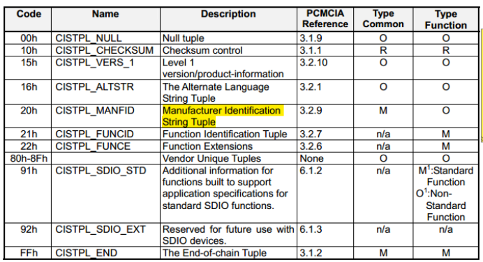
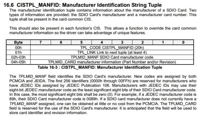
我們還是只拿一個制造商tuple code來說明下,讓你們大概知道tuple code是什么就足夠了吧