
工具說明
走線寬度是設計人員指定的一項要求,以確保走線能夠處理所需的電流容量。該工具根據以下設計規范計算走線寬度。Trace width is a requirement that designers specify to ensure that the trace can handle the required current capacity. This tool calculates the trace width based upon the following design specifications:
- 最大電流Max Current
- 跡線厚度Trace Thickness
- 最大期望溫升Max Desired Temperature Rise
此工具還計算與跟蹤相關的以下附加有價值信息。This tool also calculates the following additional valuable information related to the trace:
- 阻抗Resistance
- 壓降Voltage Drop
- 線寬功耗Trace Power Dissipation
說明
該工具基于標準文檔 [1] 中包含的公式和圖表,計算傳導給定電流所需的銅印刷電路板走線的厚度,同時保持走線本身的溫升低于指定的輸入值。
通過提供額外的輸入參數(環境溫度和走線長度),可以計算走線總溫度、電阻、電壓降和功耗(功率損耗)。
應該注意的是,由于通過空氣對流散熱,外部 PCB 層比內部層實現更好的熱傳遞。反過來說,內部電介質不能很好地導熱,這就解釋了為什么內部走線比外部走線寬。
This tool, based on the formulas and graphs contained in the standard document [1], calculates the thickness of a copper printed circuit board trace required to conduct a given current, keeping the temperature increase of the trace itself below the specified input value.
By providing additional input parameters (ambient temperature and trace length), it is possible to calculate the trace total temperature, resistance, voltage drop and power dissipation (power loss).
It should be noted that external PCB layers achieve better heat transfer than internal layers, due to the heat dissipation through air convection. The other way around, internal dielectric does not conduct heat very well and that explains why internal traces are wider than external traces.
線寬計算
First, calculate the area according to the following formula:
A = (I / (k * TRISEb))1/c (I)
Then, calculate the trace width:
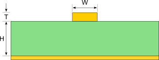
W = A / (T * 1.378 [mils/oz/ft2]) (II)
Where:
A is the cross-section area [mils2], I is the maximum current [A], TRISE is the maximum desired temperature rise [°C], W is the trace width [mils], T is the trace thickness [oz/ft2], k, b and c are constants. According to IPC-2221A Par. 6.2 (“Conductive Material Requirements”), their values for inner layers are as follows: k = 0.048 b = 0.44 c = 0.725
Equation (II) is based on a curve fit to the charts provided in [1] (par. 6.2, Figure B and Figure C).
Trace temperature calculation
The overall trace temperature can be calculated as follows
TTEMP = TRISE + TAMB
Where:
TTEMP is the trace temperature [°C], TRISE is the maximum desired temperature rise [°C], TAMB is the ambient temperature [°C].
Resistance calculation
First, convert the cross-section area from [mils2] to [cm2]:
A’ = A * 2.54 * 2.54 * 10-6
Then, calculate the resistance:
R = (ρ * L / A’) * (1 + α * (TTEMP – 25 °C))
Where:
T is the trace thickness [oz/ft2], W is the trace width [mils], R is the resistance [Ω], ρ is the resistivity parameter, whose value for copper is 1.7E-6 [Ω · cm], L is the trace length [cm], α is the resistivity temperature coefficient, whose value for copper is 3.9E-3 [1/°C], TTEMP is the trace temperature [°C]
Voltage drop calculation
Voltage drop can be calculated as follows:
VDROP = I * R
Where:
VDROP is the voltage drop [V] I is the maximum current [A] R is the resistance [Ω]
Power dissipation calculation
Power dissipation, or power loss, can be calculated according to the following formula:
PLOSS = R * I2
Where: PLOSS is the power loss [W], R is the resistance [Ω], I is the maximum current [A]
Example 1
Inputs
I = 10 A
T = 2 mil
TRISE = 20 °C
TAMB = 25 °C
L = 10 inch
Output
Cross-section Area = 256.27 mils2
Trace Width = 128.13 mil
Additional output
Trace Temperature = 45 °C
Resistance = 0.0282 Ω
Voltage Drop = 0.282 V
Power Dissipation = 2.82 W
Example 2
Inputs
I = 8 A
T = 3 oz/ft2
TRISE = 86 °F
TAMB = 27 °C
L = 10 inch
Output
Cross-section Area = 147.29 mils2
Trace Width = 35.63 mil
Additional output
Trace Temperature = 57 °C
Resistance = 0.0511 Ω
Voltage Drop = 0.409 V
Power Dissipation = 3.27
Reference
[1] IPC-2221A “Generic Standard on Printed Board Design”
- PCB線路板細節鑼槽問題的解決方法
- AD中,PCB蛇形走線超級教程
- 平基底DIP元件波峰焊氣孔不良的研究
- 插件焊接缺陷分類與機理分析
- PCB制造全制程:從設計到成品的工藝邏輯
- PCB機械物理特性
- AD中,PCB蛇形走線超級教程
- PCB材料選擇與粘接指南
- MOSFET失效分析
- 詳解PCB走線與信號完整性問題當提及到高速信號的走線的拐角角度問題,都會說高速信號不要以直角走線,要以45度角走線,并且會說走圓弧會比45度拐角更好。
- 數字微流控-電浸潤-Opendrop開源方案分析今天與各位同好分享一下前天提到的Opendrop的數字微流控電浸潤方案的分析,有些地方還是不太看得懂,也歡迎看懂的同好私信講一下看不懂部分的原理。